Step-by-Step Assembly Instructions
This step-by-step guide to building the MINT amp is only intended as guidance for experienced amp builders. Despite having a relatively simple circuit, there are some tricky parts to the actual build process. If this is your first amp, put the board away and at least hack together a quick CMoy amp to acquire some basic skills.
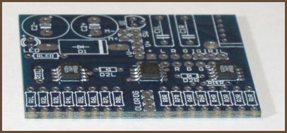
1. Add the chips
|
As a general rule, you should install the shortest components first, and on the MINT board that's the SO-8 chips. This is especially true with surface-mount components because you need to "wipe" the leads with the iron to remove excess solder. You can't do that easily if there are taller components nearby on the board.
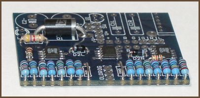
2. Add resistors and diodes
|
Add the next-taller components: the resistors and diodes. All of the diodes are optional, but I recommend that you at least add D1 (the crowbar).
If you want to add the op-amp biasing current-regulating diodes (D2), you can put that off until step 4 if you want. The same goes for the buffer bandwidth resistors (R11).
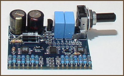
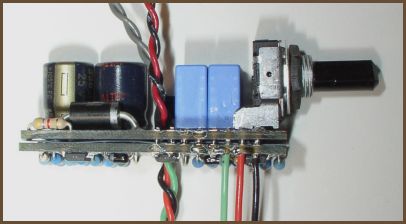
3. Add the big stuff
|
Now add the capacitors, the TLE2426, and the pot.
4. Test your handiwork
|
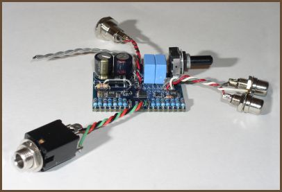
It's not a good idea to put off testing beyond this point unless you skip the next step. The reason is, once you've halved the board and reattached the two halves, tests are a bit more difficult to make and changes become very difficult to make.
I make the wires extra long and either tin the bare ends for attaching alligator jumpers, or attach temporary jacks to the ends. The idea is to make it easy to test and then easy to go from the test setup to the final enclosed amp configuration with a minimum of rework. The wires are long because you don't know exactly how long they have to be until the enclosure is set up and you don't want to have to desolder too-short wires and put longer ones in.
Here's where the wires attach:
V+, V-
For hooking up your power source. If you've only got a simple 2-wire power supply, this is where the + and - wires go.
M+, M-
If you want to do 2×9V in series or something similar, the 'M' pads are the "midpoint" connection. That is, you run the + wire from one battery strap to V+, the - wire to M-, the - wire from the other battery strap to V-, and the + wire to M+. This ties two opposite-polarity wires from the batteries together at the 'M' pads, and the outer pair goes to the 'V' pads. By using the 'M' pads, you can avoid splicing wires together by hand.
SW
For the power switch.
LED
This is not strictly a set of wire pads, because you can just place a 3mm LED here if you want. But, if you're going to mount the LED on one of your case's panels, this is where you'll run the hookup wires. The anode pad is the one closest to C2-, and the cathode is towards RLED.
IL, IR, IG
These go to the input jack. Left, right and ground.
L, R, G
There are three sets of pads marked this way.
The three pads that parallel the 'I' pads do not connect to the 'I' pads. Their purpose is to make hookup wiring simpler for those that choose to cut the board in half and mount the halves back-to-back, and who want the input jack to be closest to the "short stuff" half of the board. The idea is that you strip enough insulation from your hookup wires that the exposed part is long enough to go through both sets of holes in the board halves. Then you stick the wire in on the "short stuff" half and continue on to the 'I' pads on the other half, then solder the wires to each half of the board. This way, you can put the input jack on the "short stuff" side without having to run the wires around the back end of the board to get to the 'I' pads on the other half of the board.
The other six 'L' 'R' and 'G' pads are along the path where the signal is coming from the "large stuff" half of the board to the "short stuff" half.
It may help you to understand what all of these pads are for if you trace the signal path on the schematic. The signal enters the amp at the 'I' pads, then goes through the pot, then through the C1 input capacitor, then down to the 'L' 'R' and 'G' pads, and finally to R1 where it enters the amp circuit proper.
OL, OR, OG
These go to the output jack. Left, right and ground.
5. Halve the board and reattach the halves (optional)
|
This is one of the coolest features of the MINT board: you can cut it in half and reattach the halves using the double row of holes along the long axis. The best way I've found so far to make this cut is to use a Dremel tool with a thin cutting wheel. I recommend the No. 409 emery wheels; if you use the thicker No. 420 emery wheels or the fiberglass reinforced wheels, you're probably going to end up thinning one of the traces running along the long axis, or even cutting one entirely. Take your time with this cut, making sure to stay between the two fat traces running along the long axis.
Once the board is halved, you have to reattach the halves.
One way to do this is to use common SIP pins, since the holes are on 100 mil centers. The problem with this is that you end up with a fair bit of space between the board halves; in a mint tin, this can mean the difference between being able to fit 2×9V into the mint tin with the amp board and only being able to fit 1×9V in there. The advantage of SIP pins is that they're easy to install and they put plenty of space between the board halves so there's no worry of shorting something between the halves.
The harder way is to use wire. In the picture above, notice that the input jack wires come off the board on the same side as the output wires. You do this by stripping extra insulation off of your hookup wires and push the stripped end through the holes in both halves of the board, and then solder the wire to both halves. This runs the input lines from the "short stuff" half of the board to the "big stuff" half, where the input signal continues on to the pot and thence to the rest of the circuit. All of the other holes in that picture are joined with short sections of resistor lead clippings.
If you take the latter path, I recommend that you file the lead stubble on the bottom of each board half down a bit and then cover each half with a single layer of electrical tape. By flattening the stubble out, you ensure that there aren't any sharp bits on the bottom of each board half that will poke through the tape and short the board halves out. Another popular way to avoid electrical shorts is to put a sheet of tough plastic between the two halves; the Teflon material I sell in the store is ideal for this.
6. Encase the amp board
|
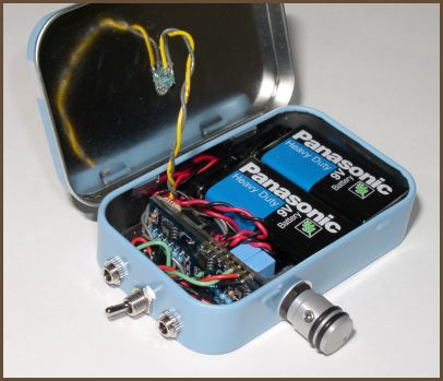
Now that the amp board is fully assembled, it's time to encase the amp. This is pretty much outside the scope of this article, but I do want to make some comments about putting the MINT into regular mint tins, since that was one of the design goals for this board.
As I hinted above, you have to keep things fairly tight inside the mint tin if you want to put 2×9V in there along with the amp board. What I do is put the I/O jacks and the switch on one short edge of the case; I use small enclosed jacks and I mount the toggle switch such that its lugs don't protrude past the end of the 1/8" jacks. This way, the plastic jack bodies keep the amp board from touching the metal toggle switch lugs, shorting something out. For the pot, I make the hole 1/32" to 1/16" bigger than it absolutely has to be so that I have enough slop to adjust the position of the board so that it fits tightly up against the jacks on the left side of the case. The pot's washer will cover up the gap between the pot bushing and the hole edge.
The only other trick to making all of that fit into a mint tin is careful routing of the extra wiring. Notice that I'm running wires in any available free space: along each side of the amp board, above the batteries, and around the rear end of the board. About the only place you have no room for wiring is directly over the top of the amp board, since that extends clear to the top of the mint tin.
7. You're Done!
|
That's it! You've got a working MINT amp!