Biasing Op-Amps into Class A
Introduction
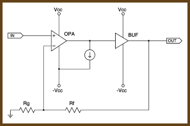
“Class A” refers to configuring an amplifier so that its output devices remain turned on all the time. This reduces thermal variation and eliminates crossover distortion, which makes the chip perform better. To bias an op-amp into class A, you simply put a current source from the op-amp’s output to one of the power rails. Everything else is details. This article is about those details.
If you want to try these ideas in a real circuit, you can leave the existing class A biasing scheme out of a PIMETA v2, and put these circuits across the Q3 positions from collector to emitter. (See the PIMETA v2 schematic.) That is, these unique parts of each biasing circuit described here go in place of the constant current symbol in the schematic at right.
This article is in some ways a history of class A biasing in the predecessors of the PIMETA v2: the META 42, the MINT, the PPA v1, the PPA v2, and the PIMETA v1. Nevertheless, these techniques are applicable to many other types of op-amp circuits.
Theory
An ideal current source is any device that will pass a constant amount of current no matter what the voltage drop across it is. Naturally, there is no such thing as an ideal current source, so this article will describe several alternatives of increasing complexity and closeness to the ideal. Most of these variations can be implemented on the PIMETA circuit board and all of them can be done on the PPA, so the text will make reference to part positions on those circuit boards.
When you put a current source on the op-amp’s output inside the feedback loop, it causes the op-amp to continuously "fight" against the current source. The chip must put out at least as much current as the current source demands in order to force its output to the voltage the op-amp inputs demand. If it did not, the current source would pull the output of the op-amp to V-. This continual fight against the current source keeps the op-amp’s output stage turned on all the time, with a constant current. Voilá, class A bias.
The reason we connect the current source to V- is that it forces the NPN transistors in the op-amp to remain active instead of the PNP ones, as would happen if we connected to V+ instead. It works either way, but in general PNP transistors don’t behave as well as NPN ones, so we’d rather make the NPN’s do the work.
The current level that must be passed by the current source depends on what load the op-amp is driving. The simple rule for this is that to keep the op-amp in class A, it has to be passing more current all the time than the load would take on its own. Imagine that the maximum signal level we expect is 3 Vrms and we’re buffering the op-amp with an Elantec EL2001, which has a minimum input impedance of 1 MΩ. The peak voltage is 4.2 V (1.414 × 3 Vrms) so the maximum current level between the op-amp’s output and the buffer is 4.2 µA, which is therefore also the minimum value for the current source.
We don’t want to make the current source value minimal, though. Down at their lower limits, transistors are nonlinear, and we’re trying to get rid of nonlinearities with this tweak. Therefore, in a buffered op-amp circuit, you usually see biases of at least 0.5 mA, and occasionally as high as 5 mA. The amount you must use depends on the op-amp and the signal characteristics; you’ll have to experiment if you want to find the optimal value.
I should repeat at this point that these numbers only apply to buffered op-amp circuits. If the op-amp is driving a low-impedance load, you will have to use a higher bias level. Imagine that the op-amp is driving 32 Ω headphones directly. The loudest signal level will likely be about 0.5 Vrms for such headphones, which means that the peak voltage is 0.7 V so the peak current draw is about 22 mA. Therefore, your class A bias would have to be higher than 22 mA to keep the chip operating in class A at all times.
It might seem from this discussion that the higher the bias level, the better. Not so. Be sure to take a look at your op-amp’s datasheet to find out its output current characteristics. If the op-amp is only capable of delivering 40 mA maximum, putting a 22 mA current source on the output of the op-amp will likely make the chip perform worse than with no biasing at all. At this level, you’re likely activating the current limiting circuitry of the op-amp, and you’re raising the operating temperature of the chip significantly. The moral of the story is that you need an op-amp capable of delivering significantly more current to the load than strictly required if you want to add a bias tweak to it.
Test Method
For all of the following methods, the test was to measure current while varying voltage across the device from 5 V to 15 V. This simulates a 10 V peak-to-peak AC signal (3.5 Vrms) between a ±10 V supply range. Few headphones require this much voltage to sound loud, but this kind of voltage requirement isn’t completely unheard of. This is also not an unreasonably high voltage value from a practical standpoint: any decent op-amp can put out this much voltage when given a ±9 V or higher supply. Finally, a high test voltage helps to differentiate the various biasing methods I test below. I’ve tested at lower voltages before, and the best methods become nearly indistinguishable at lower voltage differentials with my test equipment.
I measured the current level at three points: 5 V, 10 V, and 15 V. Then I give the current variation from 10 V down to 5 V and 10 V up to 15 V. This gives a plus/minus percent variation from the center voltage, which in an audio amp would be the same as signal ground — the “rest” point for the amplifier. You’ll notice that with most of these methods, the negative swing is worse. This is because with most current soruces, regulation improves as voltage increases across it.
Method 1: A Resistor
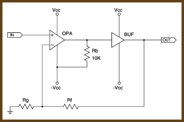
Ohm’s Law says I = V÷R. Since R is constant with a resistor, if V — the voltage drop across the resistor, in this case — is also constant, then the current through the resistor (I) is constant.
Let’s say you’re powering the op-amp from a ±12 V power supply. With no output signal, the distance will be 12 V between the op-amp’s output and V-. If you put a 10 kΩ resistor from the output of the op-amp to V-, you’ll get 1.2 mA of current draw while the output of the op-amp stays at 0.
There are two problems with trying to treat a simple resistor as a current source. First, it will only give a constant current level while the op-amp’s output signal remains constant. If the op-amp is amplifying a music signal, the bias level will only be constant during the silent parts, but the bias is there to improve the audible parts. This isn’t to say that a resistor bias is useless, just that the bias level will vary with the output signal level, which is suboptimal. With our 3.5 Vrms signal across a 10 kΩ resistor, the current level will vary by ±50%! If you’re using a battery power supply, the current variation will get worse as the batteries drop in voltage.
The second problem with this method is that the higher the op-amp’s load impedance, the better the dynamic performance of the op-amp. That’s one reason buffers help op-amps to perform better: they present an impedance in the megohms range to the op-amp. Using a resistor down in the kilohms range to bias the op-amp’s output negates this benefit.
Method Two: The Lone JFET
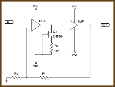
It’s not hard to fix both of these problems. A simple N-channel JFET configured as in the schematic at right is a pretty good current source.
JFETs have a property called IDSS, which stands for Current (I) from Drain to Source at Saturation. An N-channel JFET saturates when the gate to source voltage is 0 V, which you can achieve simply by tying them together. The IDSS of a JFET is a random value that falls within a particular range which you can find in your JFET’s datasheet. This range is a result of manufacturing variation, and each part will have a stable value somewhere within that range. Also, different batches of parts will tend to fall into different parts of the range.
As you add more resistance between gate and source, the voltage drop between them increases, so the current through the JFET goes down. You can use this property to tune the current through the JFET despite the wild variations in IDSS. As a bonus, adding a source resistor tends to increase the stablity of the current source as a whole.
The current through a lone JFET without a source resistor varies by -3.0/+1.6% in my test. If you add a 470 Ω source resistor, variance drops to about ±1.5% in the same situation. The other benefit of using a JFET instead of a plain resistor is that the input impedance of a JFET is up in the megohms range, so the op-amp still sees a near-ideal load situation.
Once upon a time, several semiconductor manufacturers made an encapsulated version of this circuit, called a Current Regulating Diode, or CRD. It was typically packaged in a DO-35 package like a small signal diode, though transistor type packaging was also avaialble. The advantages were that they packaged it up for you, and trimmed it, so you didn’t have to do your own JFET binning. Consequently, CRDs were fairly expensive components. Between that and the rise of digital electronics and the relative wane of analog electronics, this class of device is quite hard to find at distributors these days. Pity.
There are two new problems with using lone JFETs as current sources. (Or CRDs, for that matter.)
JFETs have a small input capacitance. This capacitance is way down in the picoFarads range, but you don’t want stray capacitance in the signal path at all if you can help it. Putting a 100 Ω to 1 kΩ resistor inline with it from the op-amp’s output will help isolate the op-amp’s output from this capacitance. (This is the purpose of R10 in the PIMETA v1 and the PPA.)
A simple JFET current source still has more variance than we want. We can do better.
Method Three: The JFET Cascode
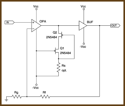
If you put a second JFET between the op-amp’s output and a JFET configured as above, you have a "cascode" configuration. (See the schematic at right.) The JFET cascode has a very interesting interaction. Q1 represents a fairly stable current bias for Q2, which means that Q2 will tend to pass a fairly stable voltage level from the op-amp’s output through to Q1. Conversely, Q1 now sees a more stable voltage than it would if it were connected straight to the op-amp’s output, so the current flowing through it doesn’t vary by as much, which helps Q2 to maintain a steady voltage level. Thus, each JFET acts to help maintain stability in the other JFET, leading to a nearly constant current level through the cascode despite input voltage variation. In my tests, current variation for a properly-configured cascode was roughly in the ±0.5% range. That’s just a few tens of microamps of current difference for 2N5484s!
A notable feature of the cascode configuration is that it will have a lower current draw than that of the Q1 alone. This can be an advantage or an annoyance, depending on your application.
If you don’t use Rs, Q2 must have a higher IDSS than Q1. If Q2’s IDSS is lower than Q1’s, Q1 will try to allow more current to flow than Q2’s IDSS value will allow; Q2 will therefore saturate, and thus it can’t do its job properly. Worse, this means Q1 can’t saturate. Neither JFET is helping the other in this situation, so the combination has about the same performance as the lone JFET (-2.4%/+1.5% in my test), only now you’re using more parts to achieve that performance level.
The simple way to ensure that your Q2 has a higher current limit than your Q1 is to use two different types of JFETs whose specified IDSS ranges don’t overlap. You could use a 2N5486 for Q2 and a 2N5484 for Q1, for example. The harder way is to buy many of one type of JFET and test the IDSS of each one, sorting them into small groups of JFETs with similar measured IDSS values. Then you pick Q1/Q2 pairs so that Q2 comes from one of the high-current groups and Q1 comes from a low-current group. The exact values don’t matter so much, just so long as Q2 is higher in value than Q1.
Now, if you add the Rs resistor, you can get away with a high-IDSS Q1, because you can simply choose an Rs value such that it forces the overall current draw of Q1 down below the lowest IDSS value that Q2 could have. For instance, suppose you were using 2N5484s. Since the IDSS range for these JFETs is 1 to 5 mA, you could pick Rs such that it would push a 5 mA Q1 down below 1 mA, so that even in the most extreme situation Q1’s current draw would be lower than that of Q2. The main downside is that this may result in an overall current draw through the cascode that’s too low to be useful. You’d have to use a JFET series with a higher IDSS than you’d normally use to work around this.
You might think that you could replace Q1 or Q2 with a CRD and get similar performance to that of a cascode, but you really need all three legs of the JFET accessible to set up a cascode. The closest you can come amounts to the same thing as a lone JFET with an Rs resistor — same topology, same performance, but with a much higher parts cost.
Testing a JFET’s IDSS
It may not be obvious how to test for IDSS from the schematics above. The way I do it is to set up a solderless breadboard (a.k.a. plugboard) with a jumper across two rows. Then I plug the JFET into the board so that the jumper connects the gate and source pins. I then connect the negative side of a ≈9 V power supply to the jumper, then connect the negative lead of a milliammeter to the JFET’s drain, and finally the positive lead of the milliammeter to the positive supply lead. The JFET saturates at its IDSS level in this situation, and that current value shows up on the milliammeter.
To get usable results from this test, your milliammeter has to have a resolution of at least 1 mA, and 0.1 mA or better is perfect. I recommend that you use a current-limiting power supply for this test because it’s very easy to short the milliammeter across the power supply with a simple slip of the probe; if your power supply is capable of putting out more amps than your meter can handle, you’ll blow a fuse in the meter. (Or if it isn’t fused, you could destroy the meter!) DMM fuses are expensive and hard to find, so you don’t want this to happen, trust me.
Once you have your breadboard set up for testing transistors, I recommend that you test a whole bag of them at once and keep them sorted somehow. That way you only have to do the test once, and then later you can pick matched Q1/Q2 pairs quickly. One way to keep your transistors sorted is to put them on a strip of tape, folded over the heads of the transistors, similar to the way some resistors and diodes come packaged. Masking tape works well for this. Another way is to get a small fisherman’s tackle box, and use each compartment to hold parts within a small IDSS range; the kind with lots of small compartments works best.
Other Resources
For another explanation of these issues, which may help your understanding, see the following post on Audio Asylum:
Op Amps Running Class A? — by Jon Risch
For an alternate explanation of the action of the JFET cascode, see section 3.06 in The Art of Electronics 2/e.
Yet another explanation of the cascode is in Siliconix application note AN103, "The FET Constant-Current Source/Limiter". Of particular value in this document is that it gives equations for determining the proper Rs value given the desired current level and the IDSS value of the Q1 JFET you’re using.